

Light powered progress



Integrated photonics uses the power of light to create energy-efficient, faster, and more accurate integrated circuits. The technology is set to play an essential role in developing solutions for scaling AI and telecommunications networks, reducing energy consumption and improving healthcare.

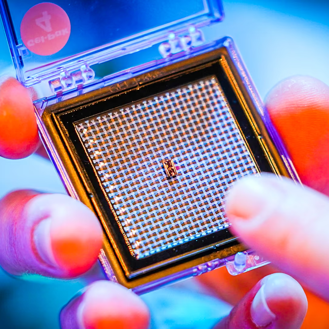


As demand for data, bandwidth and computing power continues to grow, traditional electronic approaches face increasing challenges in speed, energy consumption and scalability.
Generic photonic integration addresses these challenges by providing high bandwidth, efficient optical communication IC's via standardized manufacturing processes, delivering stable, reproducible performance at scale.
By using predefined building blocks and Process Design Kits (PDKs), designers can work at a functional level, enabling faster development cycles and more efficient design.

Indium Phosphide is one of the few materials capable of generating and amplifying light directly on a chip. This makes it uniquely suited for photonic integrated circuits that require high performance, scalability and integration.
Indium Phosphide is the only material system capable of combining all PIC functionalities: passive waveguiding, generating and amplifying light, high speed modulation and light detection into a single chip. This makes it uniquely suited for photonic integrated circuits that require high performance, scalability and integration.
SMART Photonics is a Pure-play InP foundry, manufacturing photonic integrated circuits for our customers based on their design.
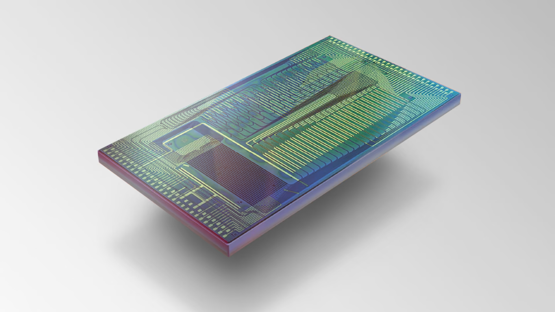
Generic photonic integration adopts the model of microelectronics in which a large variety of integrated circuits (ICs) can be made with a limited set of predefined building blocks (BBs), all fabricated using the same integration process.
SMART Photonics has developed a generic process for the production of photonics integrated circuits, in this building on the integrated photonics components research of the Technical University Eindhoven and the photonic manufacturing expertise in the Eindhoven region.
Our generic integration technology has brought about a paradigm shift in the way photonic integrated chips are produced.
In integrated photonics, a Process Design Kit (PDK) is a library of photonic components which enable designers to access a foundry's process for fabrication. The components within a PDK are the building blocks of PICs (Photonic Integrated Circuits).
When we work with our customers to create photonic chips, we make the process quicker, cost effective, and more efficient by reusing proven building blocks photonic components which have already been tried and tested. These building blocks can be assembled in different configurations to create new photonic chips.
SMART Photonics was one of the first photonics integration foundries to implement a PDK for each generation of its generic process.
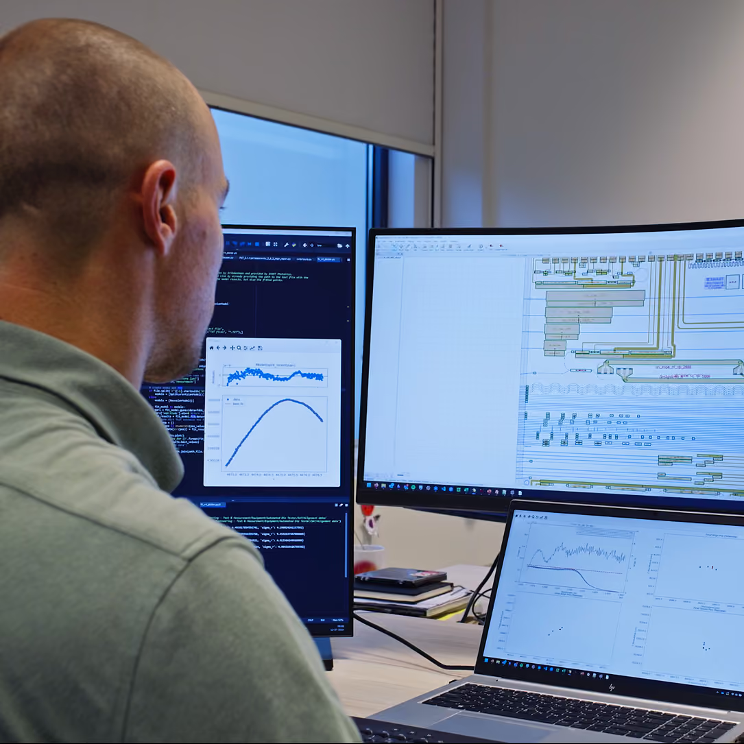

Eindhoven, where Philips started to modify light more than a century ago, has always been a frontrunner in photonics. Via SMART Photonics it resulted in a process in which optical amplifiers, modulators and detectors can be integrated with a variety of passive devices in a single chip.
As a pure play foundry we offer the complete production process of Photonic Integrated Circuits from epitaxial growth and re-growth, processing, polishing and dicing of wafers into chips. SMART Photonic is a manufacturing services supplier. As such, individual process steps, or small clusters of individual process steps like epitaxial growth/overgrowth or lithography, can be delivered.
We support our customers from the proof of concept phase up to and including full production
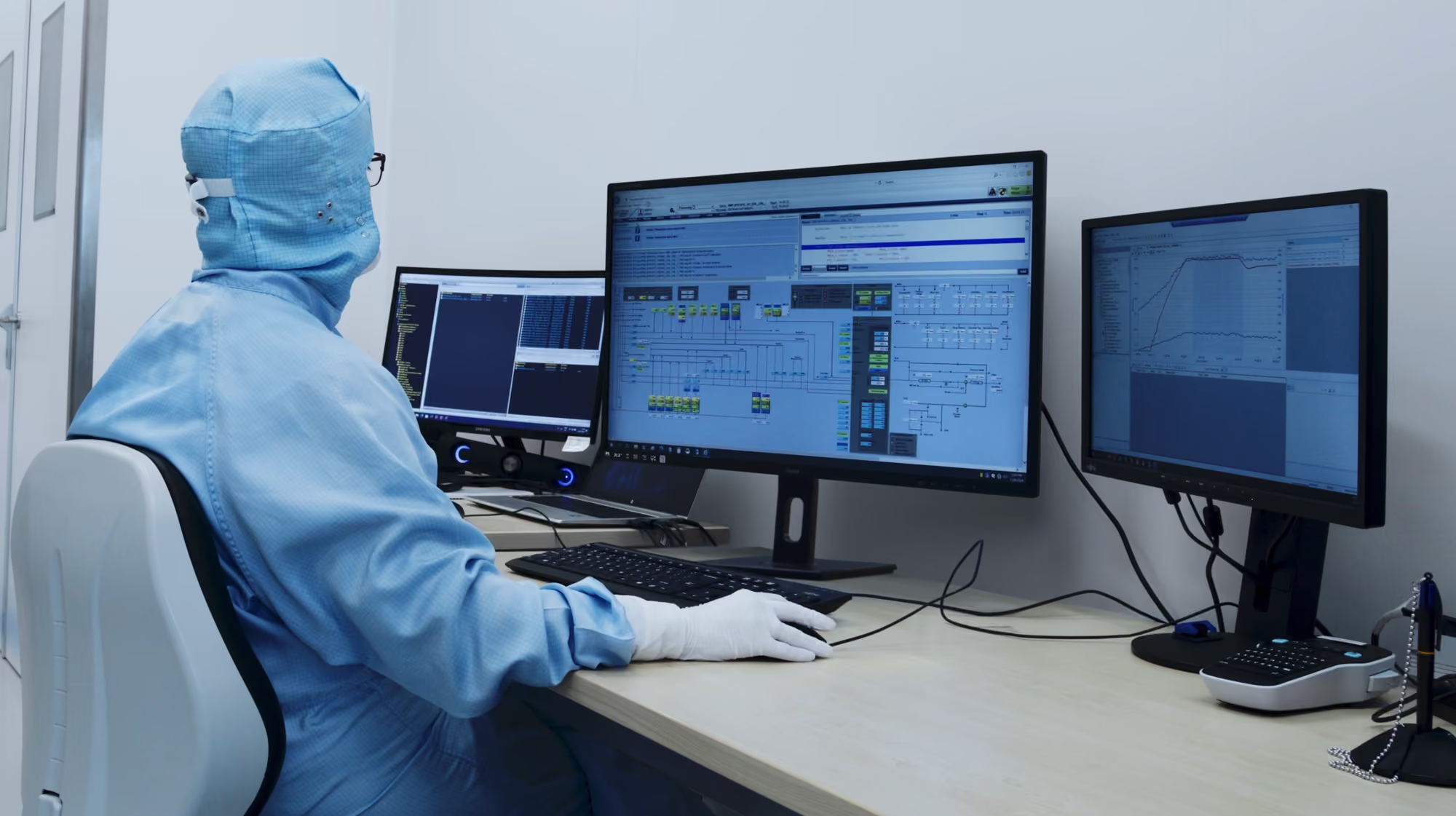
SMART Photonics has its own epitaxial growth service which is based on many years of experience. We offer base layer epitaxial growth of optoelectronic quality thin films in the InP material system. Our growth experience ranges from custom layer stacks of quantum wells, quantum cascades, and (strained) photodiodes, to the proprietary building blocks of our Generic Integration Process.
Next to our expertise in epitaxy, SMART Photonics also has invested in qualifying high-end scanner lithography for 4" InP wafer processing to replace E-beam lithography for cost reduction and throughput purposes in the volume production phase
Please contact our sales department to learn more about the SMART Photonics services or for questions.
SMART Photonics strives to be the leading foundry and development partner in integrated photonics.
We are determined to achieve the set quality objectives and committed to supporting customers and partners by providing them with products and services according to customer requirements and applicable statutory and regulatory obligations.
By incorporating our company values in our daily work, we are committed to continuously improving processes, products, services, and our management systems to enhance customer satisfaction. This commitment is supported by our ISO 9001:2015 Quality Management System certification and ISO/IEC 27001:2022 Information Security Management System certification.