As a foundry for photonic integrated circuits, we manufacture the next generation chips. Photonic chips work with light instead of electrons. The world of photonics is relatively unknown, which is why, in this blog series, we want to explain more clearly what we do at SMART Photonics. Today’s topic is about our journey to become a Tier 1 foundry.
At SMART Photonics we play a key role in technological innovation. At our foundry, we manufacture integrated photonics chips that use the power of light, resulting in energy-efficient, faster, and more accurate microchips. Separate optical components – such as a laser, modulator and amplifier – are integrated into a single compact chip, allowing previously large systems to be integrated compactly, efficiently and reliably, without the need for moving parts. These chips are essential to maintain the current rate of technological innovation. Not only in terms of technology, but also sustainability.
We have invested over €150 million in our foundry since we were founded in 2012 as a spin-off from TU Eindhoven and Philips. With the investments in our clean room, our goal is to scale up production to approximately 10,000 wafers by 2030. The production of our wafers consists of 400 steps required to build the photonic circuitry on approximately 500 chips that fit on each 100mm wafer. Establishing a foundry capable of mass-producing such a complex process while maintaining a high quality product is the main challenge that we have to overcome. Our Process Design Kit (PDK), which allows our customers to modularly design integrated photonics circuitry, has the added benefit of simplifying scaling up. Our PDK Building Blocks have been optimized for fast data communication and conversion of electrical to photonic signals and vice versa. These recent developments have laid the foundation for the next step: becoming a Tier 1 foundry.
SMART Photonics is a leading foundry in the integrated photonics industry. Our next step is to become a leading Tier 1 foundry. Not only are we confident in our ability to achieve this goal, we are well underway in the process of realizing it.
Becoming a leading Tier 1 foundry, enables SMART Photonics to do business with major Tier 1 companies in datacom, telecom, sensing (e.g. LiDaR) and MedTech. These customers typically order hundreds of wafers per year, allowing our integrated photonics chips to be implemented at scale for state-of-the-art applications. Of course, SMART Photonics – or any other chip manufacturer – doesn’t become a Tier 1 foundry overnight. It means meeting rigorous conditions in terms of quality, production capacity and delivery time.
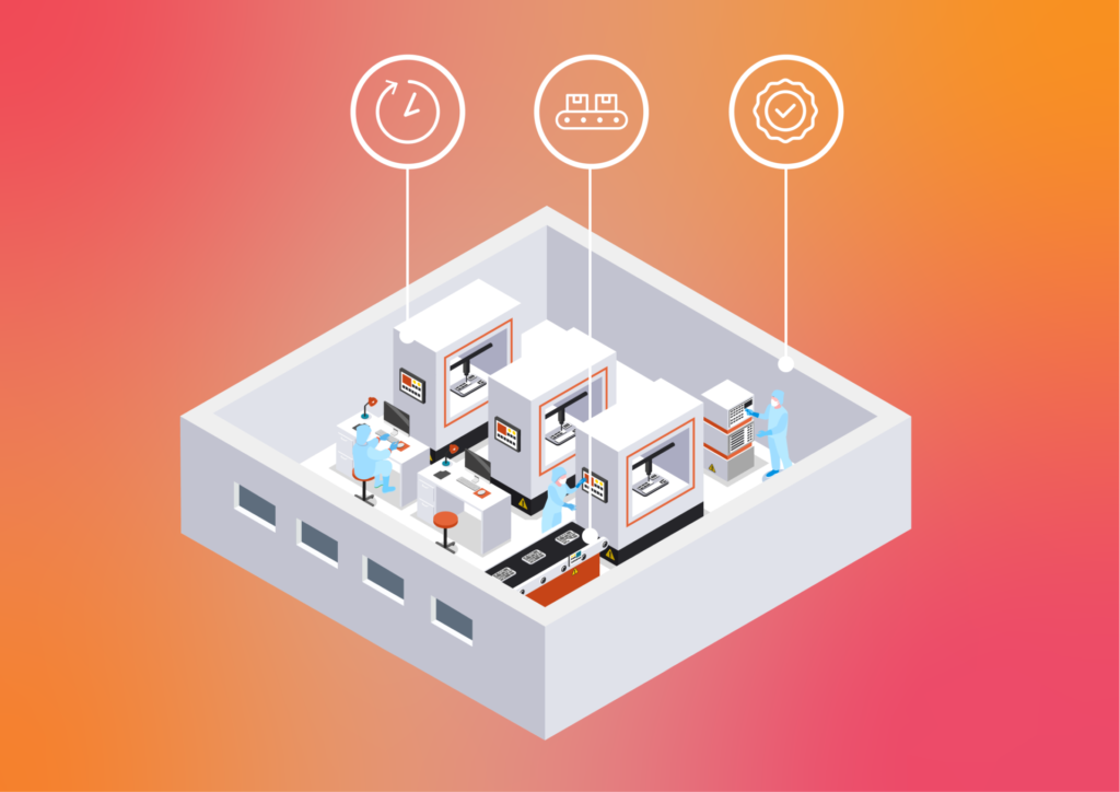
Our chips undergo rigorous endurance tests to meet reliability requirements, guarantee lifespan, and ensure we deliver quality products. We are currently processing a large number of wafers with dedicated test structures on them. As of April 1st 2024, we expanded our clean room by 40%, providing the space for our Test, Measurement & Reliability department.
Since July 2024, our processes have been compliant with ISO 9001 certification requirements, which is a great accomplishment given our complex 400-step process. This certification validates our commitment to quality and robust procedures to consistently deliver high-quality products.
It is safe to say that the entire internet runs on fiberglass connections around the globe, through data centers. Each of these connections requires a light transmitter and receiver. With the rapid development of AI, 5G and 6G, and increasing demand from hyper scalers such as Amazon, Google, Meta, Microsoft and NVIDIA, the demand for photonics chips is certain to increase massively. To realize this growth, existing data centers must be upgraded, and many new data centers will be built. Subsequently, integrated photonics are expected to account for 46% of the entire datacom market by the end of this year. As Tier 1 foundry, we must be able to meet this demand, which is why we have recently expanded our clean room. We continuously optimize our processes to improve our yield, e.g. for recurring orders. As of February 2024, we have upgraded from a 3-inch wafers to 4-inch wafers significantly increasing our chip production capacity.
The current delivery time benchmark is approximately 5-6 months. Our goal is to crush this benchmark and significantly shorten our delivery times. To achieve this, our foundry operates 24 hours a day, 7 days a week, powered by a highly educated and experienced workforce dedicated to maximizing output and quality. Moreover, we have robust redundancy equipment in place to ensure minimal impact in case of any errors. Our technology and our processes are maturing, resulting in less errors and earlier detection of process deviations.
Our next generation Integrated Photonics chips can enable and sustain innovative technological developments. We highlight some interesting applications that we expect in the future.
It is expected that data centers must become approximately twice as large to support the growth and development of AI with current technology, resulting in a 4x increase in energy consumption. Data centers are packed with hundreds of server racks, each housing many servers, all of which are interconnected throughout the entire data center. Expanding these data centers will cause problems with respect to cooling, energy consumption, and demand on the electricity grid. The only way to overcome these challenges is by using photonics chips, which allow for faster, more reliable, and more efficient transmission of signals through fiber optic cables. Also, the development of smaller data centers spread out closer to the end-user is expected, and may even be necessary. These smaller data centers will be set up to quickly solve simple, common requests, while delegating more complex problems to larger data centers.
Autonomously driving cars can use LiDAR (Light Detection and Ranging) to map their surroundings. Current LiDAR systems can amount to thousands of dollars. Good news though: LiDAR systems can be integrated directly on one optical chip, requiring fewer separate parts and eliminating the need for moving parts (e.g. rotating sensors) altogether. This results in a lower price, higher reliability and better efficiency of the system.
In the medical field, optical chips can perform non-invasive measurements within a patient’s body using specific wavelengths of light. Furthermore, our chips can measure motion and strain in large structures, such as wind turbines or bridges. The required measurement equipment would be about half the size of a shoebox as opposed to the size of a refrigerator with traditional equipment.
To realize all these steps towards a Tier 1 SMART Photonics foundry, we need a high-quality team consisting of technical experts and operators. In recent years, we have added over 100 new colleagues from across the world, bringing us to nearly 200 FTE, all committed to our vision. Expanding our high-quality team remains a challenge on our journey towards becoming a Tier 1 foundry and fulfilling our key role in the world of technological innovation. However, we are determined to overcome these challenges and continue our growth trajectory.
Our vision for the future is clear: become the leading Tier 1 foundry in photonic integrated circuits globally. We are not just building chips, we are laying the foundation of future technology. As we continue to innovate and expand, we invite you to follow us on this exciting journey, whether you are a potential partner, customer, or future team member. For a deeper dive into SMART Photonics and to follow our progress, check out this video for a comprehensive overview and stay tuned for more updates on our progress.
Check this 3 min product animation to discover how we make photonic integrated circuits.
How can you engage with our organisation and bring your bright idea to life? Check the opportunities of our Multi-Project Wafer!
MPWSMART Photonics is rapidly growing. Join us with the photonics revolution and apply now!
CareersDo you have a question or would you like to make an appointment? Send us a message!