As an independent, integrated photonics foundry, SMART Photonics has a vital role in developing next generation chips for datacom and telecom. As the digital population and the global demand for data continues to grow, so does the need for faster and more reliable networks. That’s where the original band (O-band) comes in. In this series from SMART Photonics, we aim to demystify some of the complex technologies involved with integrated photonics, and how they are helping to solve some of the world’s most pressing challenges.
In this blog post, we’ll be looking at the role of O-band in helping to meet global demands in datacom and telecom markets, what it is, and why it matters. SMART Photonics Senior Product Manager, Spiros Mikroulis shares his insights.
What Is The O-band?
The original band, or O-band, is simply the band of optical wavelengths that range from 1260 to 1360 nm. The name is derived from its status as the primary telecommunication wavelength for optical communication channels, which was defined in the mid-1970s. In those days, optical fibres had the lowest power loss within the O-band, which also provided zero chromatic dispersion – resulting in minimal signal distortion.
Although over time, the prevalence of O-band has been matched by the C-band (1530-1565 nm), the latter has higher chromatic dispersion. This causes longer wavelengths to propagate with a different velocity than the shorter ones, resulting in a pulse broadening, leading to an increased bit error rate (signal detection errors).
How It Works
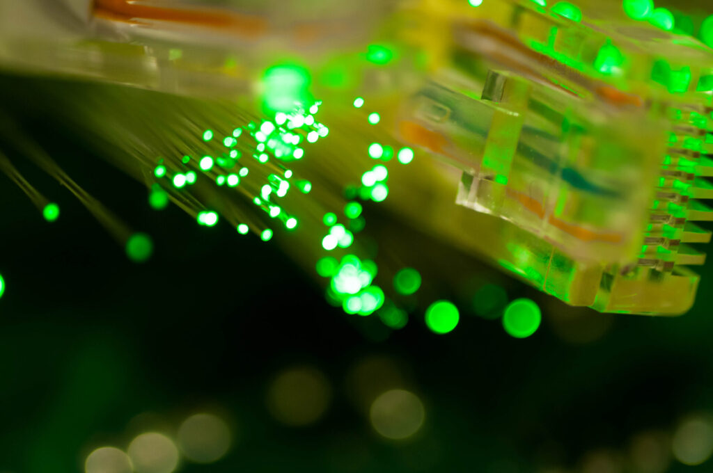
A datacom or telecom photonic chip consists of components fabricated using semiconductor layered materials that form a Photonic Integrated Circuit (PIC). It performs on/off functions (I/O) and it generates and detects photons (light).
These photons are used to transmit information – on/off data bits – via either intensity-modulation direct-detection (IMDD), or intensity/phase (coherent modulation scheme) – where on/off data is placed on time domain/phase instead of only on intensity – generated and processed in the electrical domain.
Applications In Datacom And Telecom
Due to its zero chromatic dispersion, providing a capability for high speed optical transmission rates, the O-band is commonly used in short reach/cost sensitive markets, Passive-Optical Networks (PONs) and high-speed Ethernet transmission.
Currently, the O-band is the primary choice for optical channels in the current and next generation Data Center Networking (into the data centres), where there is a high-volume demand. In the near future, we foresee two main demands for the O-band:
Current Trends In Datacom And Telecom
When it comes to the current market landscape, datacom and telecom vendors are investing in developing high bandwidth transceivers – like 50GHz, and beyond – focussing on the high speed links (50Gb/s) required to meet the demand for broadband access.
Moreover, datacom equipment providers are looking at introducing coherent technology on high capacity data centres 800G and beyond (Tb). In fact, the next step is to meet high volume demand inside the data centres, Data Center Networking (DCN) – for high-demand cloud-based applications and services (like edge-cloud).
The Benefits Of O-band
The longevity of O-band for applications in datacom and telecom is mainly due to its zero dispersion. Dispersion induces signal distortion and limits the data rate in terms of high transmission speed (gigabytes per second, Gb/s). O-band eliminates the need for, and the additional cost of, dispersion management such as digital signal processing (DSP) units. For that reason, O-band is ideally used in high-speed, cost-sensitive, high-volume markets. This helps to keep down the cost of transceivers, and reduce operational costs in terms of lower power consumption.
A Cost-Effective Solution
Currently, there is no integrated solution to address the global demands of the high speed access market, for example at the receiver stage, meeting the requirements for both high volume and low cost. Existing solutions, like highly sensitive photomultiplier semiconductor diodes named avalanche photodiodes, are not available in the required volumes, and are not re-used in relevant high-volume markets, as an example in Data Centers.
A typical solution for that would be to use the existing standard semiconductor photodiodes, simply light-sensitive semiconductor diodes, however this would compromise the system’s performance due to the increased link losses in passive optical networks. Integrated photonics can provide the answer. Without increasing the cost, photonic chips can house both an amplifier – for boosting the power of light waves – and a photodiode and provide a competitive solution that can be re-used in the Data Center market as well.
Moreover, photonic integrated circuits (PICs) not only reduce the assembly cost, they also eliminate the coupling loss of putting together the various photonic components.. By doing this, there is a direct reduction in energy consumption, which leads to savings in both energy costs and operating expenses (OpEx).
O-band + PICs
The combination of the O-band wavelength and photonic integrated circuits (PICs), fabricated on indium phosphide (InP) substrate, has two notable advantages:
First, when it comes to the introduction of new technologies like coherent – which will drastically increase the capacity of data centres – integrated photonics can address the level of complexity needed for a coherent transceiver on a single chip. Put simply, this means there is no need for additional assembly cost, and there is no need for consideration of the coupling loss on connections between multiple components.
Secondly, and most importantly, is dispersion. As already discussed, in the O-band, standard telecom optical fibre exhibits zero dispersion – minimal signal distortion – so there is no need for additional digital signal processing (DSP) which increases transceiver power consumption and cost.
Moreover, InP is the only solution that can provide monolithic integration – a complete photonic circuit or group of circuits fabricated on a single chip, that means light sources, amplifiers, modulators, detectors and passive components. Furthermore, InP has much better efficiency and performance in the O-band compared with other platforms, such as silicon photonics. An example of this is the InP optical modulator, the device that turns light into useful optical transmission bits.
Fabrication At SMART Photonics
SMART Photonics offers both Multi-Project Wafer (MPW) run and dedicated runs in O-band. This enables customers to develop, test, and scale PIC solutions and discrete components for transmitters and receivers – ensuring their products are globally competitive.
Read more about MPW Runs and dedicated runs.
Future Possibilities
SMART Photonics currently provides PIC solutions and discrete components in O-band, targeting high speed access, but we aim to facilitate the repurposing of this technology for the data centre market.
At SMART Photonics, in parallel with the O-band platform, we’re also about to release our coherent platform. To begin with, this will focus on the C-band (1530-1565 nm) but our future aim is to break the cost barrier for OEMs and vendors to offer coherent in the O-band.
Bringing together the knowledge of developments in O-band and coherent, we can help to address global needs for low energy consumption in data centres. Put simply, coherent in the O-band will lead to greener data centres.
As a pure play indium phosphide (InP) foundry, our roadmap is completely aligned with customer and market needs. Our customer-centric approach means that we strive for an ongoing collaboration in order to push forward developments which directly benefit our customers.
Right now, we’re keen to engage with customers looking to develop PICs in the O-band, not only to achieve low-cost, high-speed access but to work towards the future of more sustainable data centres.
Interested in combining the O-band with integrated photonics to help shape more sustainable data centres? Get in touch with us at sales@smartphotonics.nl
About SMART Photonics
Today, technology is everywhere around us and part of our everyday lives. Technology like integrated photonics plays an essential role in finding and developing solutions for the world’s problems, such as reducing energy consumption, improving healthcare, fighting food waste and our continuous hunger for information. SMART Photonics offers solutions for data and telecommunication, as well as for sensing – such as Lidar – and medical applications. And it doesn’t stop there.
SMART Photonics aims to improve people’s lives and create a better world with the help of integrated photonics. We are an independent foundry – producing high-end Photonic Integrated Circuits for customers. One that thinks ahead. Our goal? To always look for innovative solutions that make a difference for our customers. From proof of concept to full production. Adding value at every step of the way. And no matter what the challenge is, we make it happen.
How can you engage with our organisation and bring your bright idea to life? Check the opportunities of our Multi-Project Wafer!
MPWSMART Photonics is rapidly growing. Join us with the photonics revolution and apply now!
Careers
Do you have a question or would you like to make an appointment? Send me a message!