Transition from 3 to 4 inch doubles the production capacity, accelerating the commercial roll out
SMART Photonics is taking an important step in becoming the leading foundry for next generation chips. The Dutch foundry has significantly scaled up its production of photonic chips (PICs) by transferring its entire production capability from 3-inch to 4-inch wafer substrates. Confirming its technology leadership, SMART Photonics is one of the first integrated photonics foundries offering 4-inch InP wafer production. The resulting doubling of chip production volumes accelerates the commercial roll out of the foundry’s photonic chips.
The worldwide demand for photonic integrated circuits is expected to grow by double digits for years to come. The main drivers for this growth are Telecom 5G/6G applications and Data Center upgrades to 800Gb/s and beyond, in order to get ready for AI (Artificial Intelligence). New developments such as LiDAR in the automotive industry, and Quantum Key Distribution as an enabler for advanced internet security, will also play a key role in driving the volumes up.
“Purchasing, installing, testing and qualifying the new 4-inch processing equipment was a huge effort, so we are very excited that we have succeeded in taking this important technological step forward.” said Guy Backner, Chief Operating Officer of SMART Photonics.
“It’s not just about the sheer number of wafers produced; the larger wafer substrate will now enable us to better meet the number of optical chips needed in the market, which will help us to fulfil our ambition of becoming a world-leading foundry in integrated photonics.”
In July 2023, SMART Photonics secured funding of €100M from strategic industry and financial players such as chip equipment giant ASML and chipmaker NXP. The funding included €60M in public financing as part of the PhotonDelta approved National Growth Fund project. This latest round of funding enables SMART Photonics to accelerate its development, strengthen its Process Design Kit capabilities and extend its manufacturing base as the company continues to mature.
The 3 to 4-inch transition was made possible as well thanks to the support of the European Union’s Interreg North-West Europe project “OIP4NWE” (NWE 758).
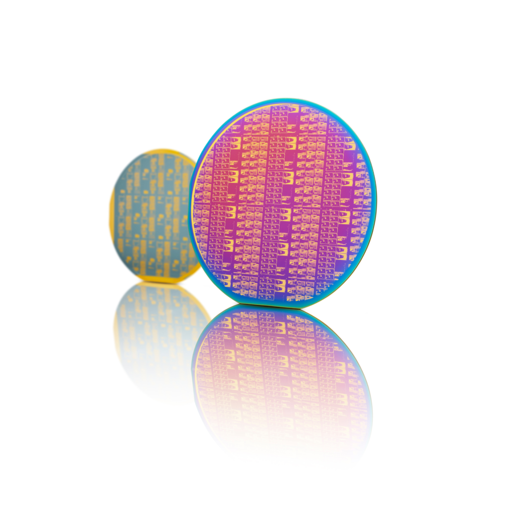
![]()
Picture on the right:
4” wafer including PhotonFirst designs, processed within the OIP4NWE project
How can you engage with our organisation and bring your bright idea to life? Check the opportunities of our Multi-Project Wafer!
MPWSMART Photonics is rapidly growing. Join us with the photonics revolution and apply now!
CareersDo you have a question or would you like to make an appointment? Send me a message!